|
|
|
 www.design-reuse-embedded.com
 |
|

NoC Interconnect Fabric IP Improves SoC Power, Performance and Area
by Charlie Janac - President and CEO of Arteris and Monica Tang - Applications Engineering Manager at Arteris, Jan. 14, 2016 –
Imagine you have defined the structure of a system-on-chip and now you have to assemble all the IP blocks and make them communicate on the die. You have spent months rigorously selecting SoC IP that reflects the desired chip functionality. However, without the on-chip interconnect fabric it is just a collection of isolated blocks. The blocks become a final SoC architecture only by the addition of communication pathways. It is the on-chip interconnect and the quality-of-service, communications features and topology that ultimately implement the architecture, structure and capabilities of a system-on-chip.
Virtually all high-volume mobility and multiprocessor systems in production today use network-on-chip (NoC) technology. That is because it is the most efficient way to make SoC blocks communicate. The increasing complexity of SoCs has driven the adoption NoC interconnects. SoC complexity has advanced in several dimensions:
- Smaller critical dimensions:
- New SoC design starts in 40nm are tapering off, 28nm and 16/14nm are popular, and some current mainstream designs are now under way in 10nm and 7nm.
- Density increases 25x between 65nm and 10nm, reaching 16M gates/mm2.
- Die size has tended to stay the same as node size decreases, meaning more IP is getting placed in an average SoC with each process node change.
- The number of IP blocks is increasing to several hundred for leading edge SoCs.
- A die of 8 mm x 8 mm has a theoretical billion gate capacity in 10nm.
- Small SoCs have grown in power management complexity as IoT applications require multi-week or even multi-month battery life.
- Interconnect IP speed requirements have increased in some applications to well over 1GHz.
- Multiple interconnected NoC pathways are needed to satisfy intense data bandwidth requirements.
This increase in complexity has led to swelling industry-wide adoption of NoC interconnect IP due to its inherent architectural advantages in power consumption, performance, and area over traditional crossbar and bus-based interconnect technologies. These advantages enable SoC architects and designers to cope with the growing complexity of heterogeneous architectures while reducing both the research and development and unit costs.
Arteris pioneered NoC interconnect IP in the mid-2000s, and has considerable experience helping users improve the performance, power and area profiles of their SoCs. Along the way, users have asked for, and received, hundreds of features needed to effectively design various types of differentiated SoCs ranging from the lowest cost to the most complex.
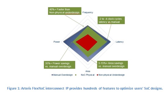
The goal of many of these features is to improve the power, performance and area (PPA) of the interconnect IP in order to achieve both research and development and unit cost savings. They can also help improve SoC IP assembly productivity. By examining some of the power, performance and area features of NoC interconnect IP, it will become evident how these enhancements were achieved.
Power Consumption
NoC technology offers more than 7 times idle power reduction versus a hybrid bus or crossbar interconnect. Here's why:
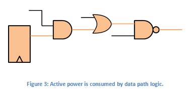
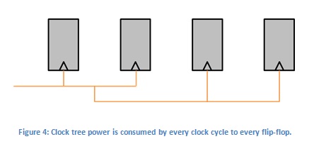
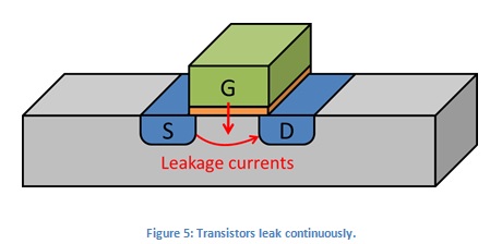
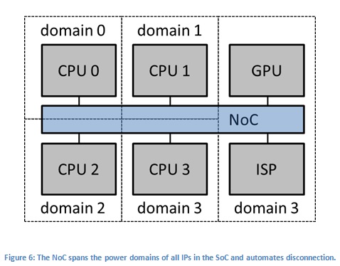
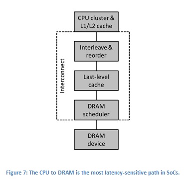
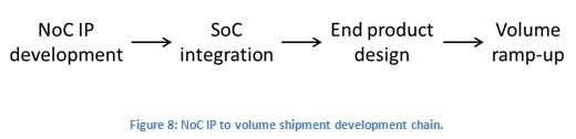
Active power is used by CPUs, GPUs, multimedia subsystems, communications subsystems, and other IPs when they are busy and generating data traffic. Use case operating modes and data sets determine whether these units are operating at peak levels or at reduced frequency and voltage levels. Clock tree power is consumed by IP blocks when they are enabled and being clocked, regardless of their activity level, and whether they are busy processing data. Interconnect IP makes a significant difference in clock tree power consumption, which tends to dominate active power as a portion of the total power consumed by a system averaged over extended periods of time. SoC power is not simply based on IPs being on or off. Various parts of the SoC become active in different use cases, causing combinations of IP blocks to consume in a range between full active power and clock tree power only. Leakage power is consumed by each transistor in a chip when it is powered on. LVT (Low Voltage Threshold) logic cells run fast, but have higher leakage than other cell types. Many chip designs use a mix of cells, and choose LVT cells only for the paths that have trouble meeting timing requirements. One way NoC IP helps to minimize leakage power is by enabling a chip design to need fewer LVT cells. The NoC does this by selecting optimal physical locations of pipeline stages within the die floorplan. Optimal physical location of pipe stages avoids wire capacitance and long propagation delay that creates troubled timing paths. During times of high data processing throughput in CPUs and GPUs, leakage power consumption is minimized if the processor runs as fast as possible to complete its task before powering down. To achieve this, it is key for the NoC to supply the high bandwidth required. Once a processing task is complete, the NoC is a mechanism for safely shutting down power domain sections of the SoC as they are unneeded. In conjunction with the SoC power controller, the NoC interconnect is an active participant in lowering active power. The Arteris' FlexNoC interconnect IP, for example, does not itself, reside in its own power domain. It resides within the power domains of IPs in the SoC and allows for the automated creation and configuration of power domain adapters and asynchronous clock domain crossings inside the interconnect logic itself. Proper handling of IP shutdown and disconnect is critical from an interconnect point of view. Messages can continue between active units but must be prevented from traveling to powered-down IP blocks. Making power-down safe helps programmers achieve maximum power reduction, such as in the the ultra-low power consumption use cases required by IoT chips to extend battery life. With efficient power domain management, clock tree power is the main determinant of both battery life and heat generation for mobility, consumer, IoT, server, and storage array SoCs. Whereas logic gates contribute to leakage, register flip-flops and wire capacitance determine clock tree power. It is important to design with minimal register state redundancy and minimal long-wire routing in the floorplan for any given SoC functions. Wires cost buffer cells. Each wire requires a large buffer every 100 microns or so to handle increasing RC effects. Clock Gating Another key aspect that greatly reduces clock tree and register power is clock gating. It is desirable not to toggle clock tree wires twice per clock cycle when clock control methods can detect that registers will not toggle. An advanced NoC IP supports three levels of clock gating, to minimize power consumption significantly. At the cell level, synthesis gates flops such that clock tree leaves will not toggle. That clock gating logic is localized within small groups of flops, and its application is limited by the area overhead of additional clock gating logic. The NoC gates entire branches of the clock tree at a per unit level. Each unit, when not processing a packet, is completely clock-gated. Only parts of the NoC that are processing data receive clock edges. These techniques cover a large majority of the clock tree, but are automatic and outside of the control of software. At the highest level, software can take advantage of units that support power-down to ensure safe gating of the entire clock tree to large portions of the NoC. This does not have the benefit of eliminating leakage power, as do power-down methods, but allows much faster wake-up from a clock-gated low power mode. "On-the-fly" clock gating wakes up within the clock cycle, so there is no negative impact on throughput or latency. As a result, a large majority of the interconnect logic is gated off, even when a processor is thrashing the DRAM during an operating mode. These features greatly reduce clock tree and register power. Leakage power consumption is worsened by place and route wire congestion points causing higher wire-capacitance per cell and therefore requiring high speed/high leakage cells. Hybrid buses and crossbars use large centralized routers which cause congestion points in the layout. Virtual channel networks add gratuitous islands of buffers and flow control logic. By contrast, NoC interconnect logic is distributed, eliminating congestion points and lowering leakage power consumption. Furthermore, it allows each link to be configured separately for the optimal quality-of-service. Overall, the features in NoC greatly reduce SoC power consumption. Performance, Bandwidth and Latency NoC technology allows designers to optimize SoCs for three often-competing metrics: Multi-gigahertz frequencies, controllable latency for all NoC IP connections, and scalable bandwidth by individual trace. The following unique aspects of NoC technology enable this optimization: Packetized communications. Transaction requests and responses are packetized at IP interfaces, enabling a NoC to run at higher frequencies than a hybrid bus or traditional crossbar, and offer higher data capacity per wire. The maximum frequency is limited only by the physical constraints of fab process technologies. One NoC was clocked at 1.6GHz in a popular chip fabricated in a 28nm TSMC HPM process. Scalable bandwidth. Having exactly the bandwidth required for a particular application and mode is a highly desirable feature. That means designing a chip to use minimum wire, gate, and register hardware resources to achieve a throughput goal. Some connections need very high bandwidth, and may use up to 1024 bit wide links. Connections running at 1.6GHz frequency over 1024-bit links provides more than 1 terabyte of bandwidth per connection. High-end gaming and automated driving assistance systems (ADAS) SoCs often require this level of high throughput. Most types of systems have more typical bandwidth requirements and use 32-, 64- and 128-bit connections, while some require only low bandwidth, sufficiently provided by 8- and 16- bit connections. Controllable latency. The Arteris NoC interconnect needs one cycle or less for packetization to get transactions onto the efficient transport network. The latency of packetization logic is almost insignificant, and pays ample dividends by the ability to run a fast transport network. Zero latency NoC capability places the packet header in parallel with the payload to eliminate any header latency penalty. This capability is used selectively for individual latency sensitive connections. On the contrary, hybrid busses carry control and address information alongside data for every connection. Because hybrid busses have multiple layers, large cross bars, and more logic, their overall latency performance is worse than NoCs. There are, however, latency insensitive connections, such as I/Os, that are only used on SoC bring up. For these types of connections, latency is not critical, and so wire conservation is possible. An 8-bit wide path that processes packet headers and payloads over several cycles trades latency for wire conservation. An effective NoC interconnect IP allows a wide range of trade-offs between high frequency, bandwidth, and number of wires used. Die Area NoC technology offers die size reductions of 1-to-4 mm squared compared to hybrid buses or other inefficient interconnect implementations. Because NoC interconnects serialize communication into configurable bus widths, they route large packet throughput on a small number of wires. Bandwidth is flexible, and managed by configuring the appropriate bit width from 8 bits for I/O IPs to 1024 bits on the high end. In the Arteris NoC, packetization takes place at IP interfaces which are the edges of the interconnect network so that the core logic is simple and fast. This also conserves gates. Compared to hybrid busses, NoC interconnects have 50% of the total wire length and 30-50% fewer gates. Interconnect IP typically represents 8-12% of SoC area. However, if poorly designed, it can consume over 30% of SoC power. Saving 50% of Interconnect IP area saves about 3mm squared of silicon area in typical SoCs. At a 28nm process node, each 1mm squared of silicon cost around 10 cents. That is a cost saving of 30 cents per chip. At a volume of twenty million units, $6M would be saved over the production life of an SoC. Across a family of 5 such SoCs, your savings are $30M, and even more if the volumes are higher. This is why NoC Interconnect IP has been rapidly adopted by the majority of leading SoC design teams, and is almost certainly in the cell phone or tablet you are holding right now. State of the Art in Interconnect IP Technology Beware: Not all NoC interconnects are equal. It is a complex technology that requires partner participation, multi-disciplinary product development, and a lot of time and capital to meet the needs of the ever-evolving SoC designs. It takes time to develop a NoC interconnect product, prove it on successful initial projects, get those designed into end-user systems, and have those ramp up to high volume shipments. Meanwhile, it requires flexibility, a broad understanding, and routine releases to keep up with the evolving requirements of leading edge SoC design teams. Conclusion NoC interconnect IP offers a number of advantages for SoC power, performance and area. There is no cheating Mother Nature, but NoC interconnect exploits her leniencies. With effective design, NoC interconnect IP enables efficient optimizations between power, performance, and area for the entire SoC.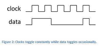
 Contact Us