|
|
|
 www.design-reuse-embedded.com
 |
|

EnSilica opens specialist Design Centre for RF and low power sensing applications based near Oxford
Wokingham, UK, Oct. 25, 2016 –
EnSilica, a leading independent provider of semiconductor solutions and IP, has further expanded its network of specialist design centres with the establishment of a new facility near Oxford (UK) focusing on RF and low power sensing applications.
The new RF and low power sensing design centre will be headed up by Alan Wong, formerly the IC Design Director at Frontier Microsystems, who joins EnSilica with immediate effect as Director of RF IC Design. Alan brings with him a design team whose pioneering experience in ultra-low power RF and sensor interfaces significantly extends EnSilica's skills-base in addressing the needs of wireless connected IoT and wearable products.
"With their expertise covering Bluetooth low energy (BLE), near field communications (NFC) and other proprietary technologies, we are extremely pleased to welcome Alan Wong and his team to EnSilica," said Ian Lankshear, CEO of EnSilica. "With the team's proven track record of successfully delivering class-leading low power wireless SoCs and IPs for wireless personal area networks (WPAN), digital broadcast, medical bio-telemetry and other consumer applications, our new RF and sensing applications design centre has an instant head start in the market."
The establishment of the new RF and sensing design centre grows EnSilica's headcount to 74 staff over four design centres with around ten per cent of the staff having PhDs. It also complements EnSilica's existing headquarters design facility in Wokingham (UK), specialist analog and mixed-signal IC design centre in Bristol (UK) and specialist design and functional verification capabilities in Bangalore (India).
"The opening of our new RF and low power sensing applications design centre near Oxford (UK) is a significant step forward in the ongoing development of our semiconductor design and supply business. It perfectly complements and further extends our existing end-to-end ASIC design capabilities, including systems design, mixed-signal and digital design, embedded software, and operations, to provide us with flexible and scalable RF and sensing design expertise for IoT projects requiring custom ASIC development," concluded Ian Lankshear.
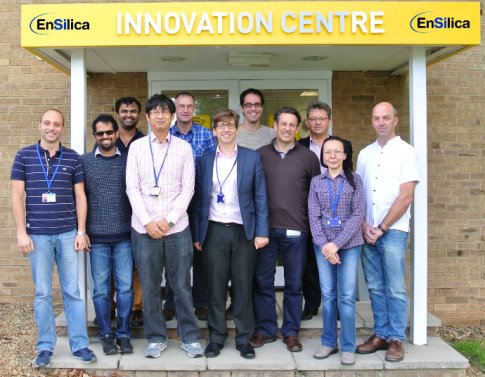
EnSilica's RF and low power sensing design team with Ian Lankshear, EnSilica's CEO (centre, front row) and Alan Wong, EnSilica's new Director of RF IC Design (third from left, front row)
About EnSilica
EnSilica was founded in 2001 and has a strong track record of success in delivering ASIC and FPGA-based solutions to semiconductor companies and OEMs worldwide. The company is headquartered in the UK and has subsidiaries in India and the USA. The company is a specialist in low-power ASIC design and complex FPGA-based embedded systems. In addition to supplying IP and turnkey ASIC/FPGA development and supply, EnSilica also provides point services to companies with in-house ASIC design teams. These services include system engineering, analog and mixed signal design, and advanced verification using UVM, DFT and physical implementation. For further information about EnSilica, visit http://www.ensilica.com.
 Contact Us