|
|
|
 www.design-reuse-embedded.com
 |
|

Solving the problem of growing ASIC respins

By Kava_Staff - Thalia Design Automation Blogs, Nov. 12, 2020 –
Semiengineering.com recently reported on an industry survey showing an increase in respins due to analog circuitry failing or falling out of operable range.
The reasons behind this trend are complex, but the article suggests it comes down to analog tuning - the process of tweaking a design to maximise performance while staying within the operational parameters of the overall circuit. The article also explains that the chief scientist at Mentor, a Siemens Business, analysed the results to determine the scale and scope of this trend - whether it was affecting newer designs on the latest technology nodes, or if it was a universal problem.
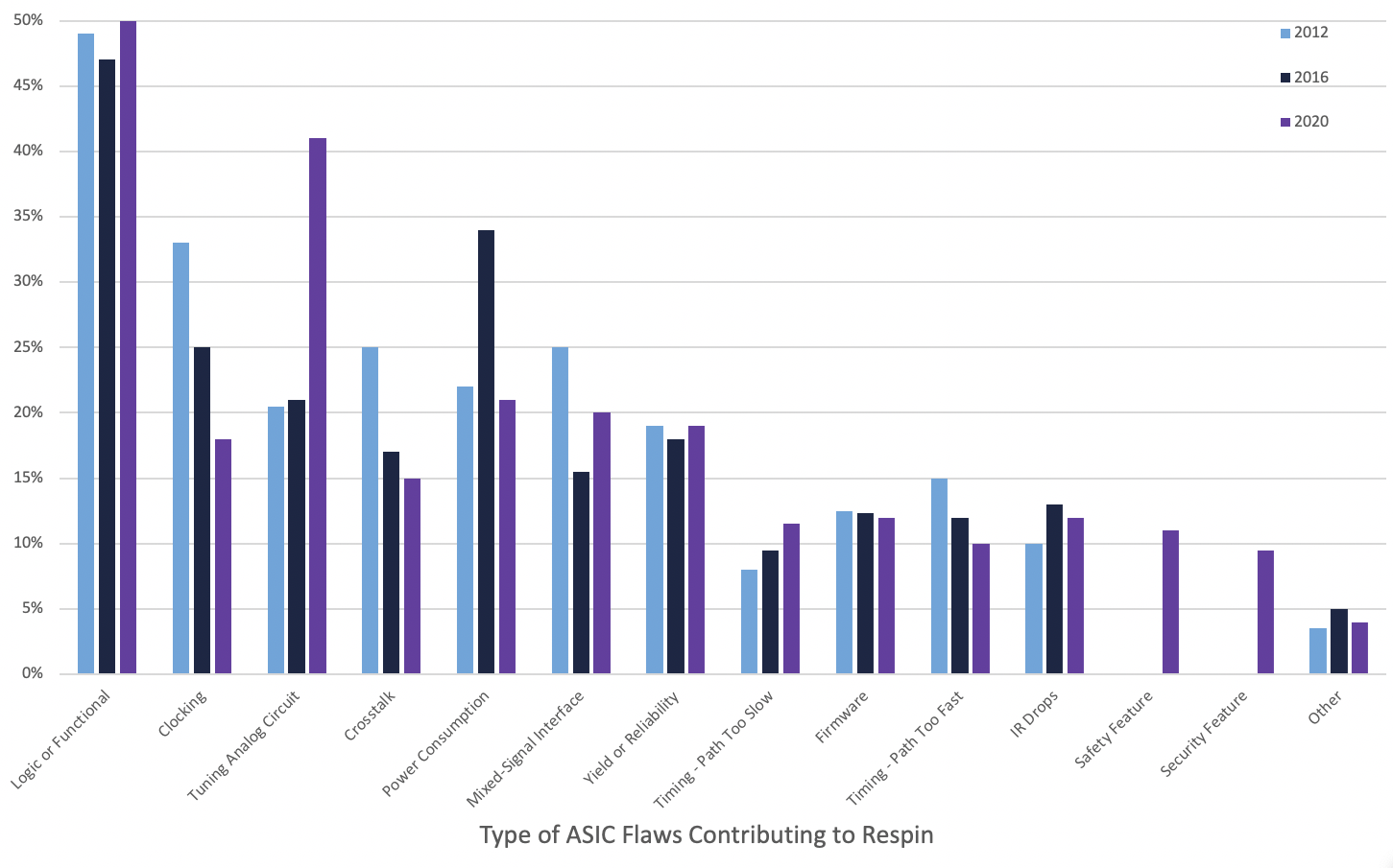
It would be easy to assume that the problem was relating to newer nodes and newer processes, but on review, the issues are affecting technology nodes from sub-7nm to 150nm and higher.
So what's causing the increase in failures?
Put simply, the complexity of new devices. The number of complex devices is growing, and is set to continue with the expansion of the IoT. Automotive components are also massively on the rise, both in number and complexity, thanks to the developments towards self-driving cars. Companies are trying to fit all circuitry on the same substrate or on a single technology node and schematic simulation isn't able to accurately assess function and full parameters.
There will always be issues arising when working with new nodes and there is a learning curve for design teams to fully come to terms with the limitations, issues and particular traits displayed by these new nodes. Implementing this knowledge into toolsets is only achievable once they are fully understood. But if that learning curve therefore involves respins and 'back to the drawing board' moments at increasing frequency, then time to market will be affected for new devices. And increasing time to market for a new chip in a competitive industry can be the difference between market success and failure. Second place really is the first loser.
As IP reuse specialists, this is not news to us. We have worked with many clients evolving analog IP from one technology to another or even from one foundry to another. Most engagements are accompanied with the need to improve power consumption, speed, performance or the physical size of the silicon chip, and when these needs are implemented, they have knock on effects to other characteristics, resulting in the silicon not performing to specification.
We know this; it's what we do. It's why we developed our technology analyzer to be able to identify differences between base and target technologies and highlight where a circuit will fail. Our Trifecta, including the AMALIA platform, helps to identify the root cause of an issue and allows our design engineers to nudge a design back into specification before migration; mitigating the need for respins for out-of-tolerance circuits.
As experts in reusing analog IP on different process nodes or technologies, we've spent years developing processes to ensure IP works as expected and as needed in target technologies. We do this by deploying our Trifecta - advanced development methodologies, the targeted automation of our AMALIA platform and our design expertise. Using this Trifecta approach means we can verify IPs and their behaviour or performance before migration. Part of the AMALIA platform uses our proprietary technology analyzer to rapidly identify parameters in both base and target technologies to identify issues, allowing our expert designers to tweak characteristics and knock the design into specification.
This methodology, used by us across multiple technology nodes and foundries, has the potential to play a significant role in the fast and efficient migrating of analog IP for the ever-increasing number of IoT, mobile and handheld devices. Analog components sit alongside digital and ensuring everything functions as it should is key in getting new products to market ahead of the competition.
 Contact Us