|
|
|
 www.design-reuse-embedded.com
 |
|

40 GHz VCO and Frequency Divider in 28 nm FD-SOI CMOS Technology for Automotive Radar Sensors

Sept. 06, 2021 –
Giorgio Maiellaro1, Giovanni Caruso1, Salvatore Scaccianoce1, Mauro Giacomini2 and Angelo Scuderi1,*
1 STMicroelectronics, 95121 Catania, Italy; giorgio.maiellaro@st.com (G.M.); giovanni.caruso@st.com (G.C.); salvo.scaccianoce@st.com (S.S.)
2 STMicroelectronics, 20864 Agrate Brianza, Italy; mauro.giacomini@st.com
* Correspondence: angelo-apg.scuderi@st.com; Tel.: +39-09-5740-4135
Abstract: This paper presents a 40 GHz voltage-controlled oscillator (VCO) and frequency divider chain fabricated in STMicroelectronics 28 nm ultrathin body and box (UTBB) fully depleted siliconon-insulator (FD-SOI) complementary metal-oxide–semiconductor (CMOS) process with eight metal layers back-end-of-line (BEOL) option. VCOs architecture is based on an LC-tank with p-type metal-oxide–semiconductor (PMOS) cross-coupled transistors. VCOs exhibit a tuning range (TR) of 3.5 GHz by exploiting two continuous frequency tuning bands selectable via a single control bit. The measured phase noise (PN) at 38 GHz carrier frequency is -94.3 and -118 dBc/Hz at 1 and 10 MHz frequency offset, respectively. The high-frequency dividers, from 40 to 5 GHz, are made using three static CMOS current-mode logic (CML) Master-Slave D-type Flip-Flop stages. The whole divider factor is 2048. A CMOS toggle flip-flop architecture working at 5 GHz was adopted for low frequency dividers. The power dissipation of the VCO core and frequency divider chain are 18 and 27.8 mW from 1.8 and 1 V supply voltages, respectively. Circuit functionality and performance were proved at three junction temperatures (i.e., -40, 25, and 125 °C) using a thermal chamber.
1. Introduction
The high pressure for realizing a low-cost, low-power, highly integrated radar system-on-chip (SoC) featuring digital processing functionalities establishes the way for advanced deep-submicron CMOS technologies, which allow for the design of millimeter-wave (mmwave) front-end circuits embedded with a high-performance digital signal processor, high-resolution analog-to-digital converters, and high-speed baseband to radio frequency interfaces, together with memory [1–3].
Modern radar sensors are based on a frequency-modulated continuous wave (FMCW) transmitted signal, whose characteristics such as linearity, modulation bandwidth, chirp duration, and PN are key parameters to determine range, velocity, and angle estimation of surrounding objects, complying with an advanced driver assistant system and autonomous driving requirements [4]. In that context, the design of the VCO is crucial for most of those parameters. The modulation bandwidth is covered by the analog-continuous VCO tuning range; a radar system with a range resolution as low as 10 cm, that is, a typical value of medium- and short-range radar, requires a modulation bandwidth of 1.5 GHz. However, the design of a wide tuning range VCO is detrimental for phase noise performance. The transmitted out-of-band phase noise that becomes decorrelated phase-noise (DPN) when reflected by a close target, i.e., bumper, which limits receiver sensitivity [5]. DPN increases the noise for a high value of intermediate frequency, limiting the maximum range of the long-range radar system.
This paper describes the design and performance of a VCO designed in 28 nm UTBB FD-SOI CMOS technology. The core has been designed at 40 GHz to optimize the resonator quality factor; it can be followed by frequency doubler to synthesize the operating frequency for medium- and short-range automotive radar sensors.
The paper is organized as follows. Section 2 describes the technology features and advantages related to the bulk CMOS. Section 3 deals with design strategies for both VCO and frequency divider, while experimental results are reported in Section 4 with state-of-the art comparison. The conclusion and comments are provided in Section 5.
2. The 28 nm UTBB FD-SOI CMOS Technology
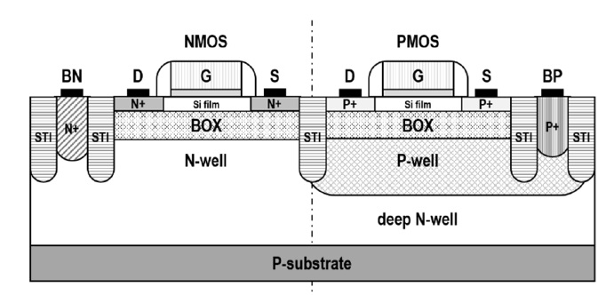
The 28 nm UTBB FD-SOI CMOS technology is one of the most promising technologies for developing high-speed, low-power analog and digital circuits, as well as radio frequency (RF) and mm-wave circuits. The technology adopted features high-k metal gate transistors fabricated on ultrathin silicon film (7 nm) sited above a thin (25 nm) buried oxide (BOX) layer, as shown in Figure 1. Owing to the ultrathin silicon film, the source and drain are isolated. The transistor channel is fully depleted, hence neither channel doping nor pocket implant are required. The thin BOX layer beneath the transistor channel acts as a second gate oxide and the N-well and P-well regions as additional gate terminals (i.e., back-gate terminals). These back-gates allow transistor threshold voltage (VT) to be properly adjusted through a wide range of body bias (BB) voltage [6–9].
The technology features two different transistor designs: conventional‐well regular‐VT (RVT) and flip‐well low‐VT (LVT). RVT transistors can adopt a reverse body‐biasing(RBB) technique to increase threshold voltage, thus reducing leakage current. In contrast, LVT transistors can use a forward body‐biasing (FBB) technique to reduce threshold voltage, thus increasing switching performance at the cost of a higher leakage current. As previously demonstrated in [10–13], body‐biasing techniques have been profitably used for compensating process, voltage, and temperature (PVT) variations, and for tuning circuit performance. Two gate oxide options are available for both RVT and LVT configuration. A thin gate oxide (1.3 nm) transistor has a nominal gate length and supply voltage of 28 nm and 1 V, respectively. A thick gate oxide (3.4 nm) transistor has a nominal gate length and supply voltage of 90 nm/130 nm and 1.5 V/1.8 V, respectively. The technology process also provides an accumulation MOS varactor (A‐MOS) [14], and metal‐oxide–metal (MoM) and metal‐insulator–metal (MiM) capacitors with 6 and 16 fF/μm2, respectively. The technology process has a low‐k BEOL with eight or ten copper layers along with a top aluminum (Alucap) layer.
 Contact Us