
Industry Expert Blogs
|
|
Minimize Design Risk and Achieve First-Pass Silicon Success on TSMC's N3E ProcessHezi Saar , Josefina Hobbs - Synopsys, Inc.Jul 19, 2023 |
Although the path from chip design to tape-out was never an easy one to navigate, this journey has become ever more challenging due to a growing demand for lower-power, higher-bandwidth applications. Indeed, chip architectures continue to increase in complexity on the most advanced FinFET nodes as billions of transistors are packed into smaller, denser silicon packages to meet new power, performance, and area (PPA) requirements. That's why Synopsys and TSMC continuously collaborate to deliver the chip design industry's broadest silicon-proven IP portfolio on the latest process technologies.
Synopsys' IP silicon success for the TSMC N3E node�which provides a fast path to TSMC N3P, N3AE, and beyond�minimizes integration risks and accelerates time to market. Read on to learn how Synopsys IP enables semiconductor companies to develop advanced SoCs and multi-die systems for a wide range applications and technologies including artificial intelligence (AI) and machine learning (ML), high-performance computing (HPC), and mobile.

Leveraging the Semiconductor Industry's Broadest TSMC N3E IP Portfolio
The explosion of data that defines the zettabyte age requires sophisticated semiconductor IP capable of handling the lowest latency operations and fastest transfers within a power-efficient envelope. From purpose-built AI accelerators and advanced driver assistance systems (ADAS) to hyperscale data centers and high-resolution displays, Synopsys Interface and Foundation IP on TSMC's N3E process is helping chip and system designers streamline integration and reduce development cycles.
Adopted by leading semiconductor companies, Synopsys IP on TSMC's 3nm process can be paired with TSMC-certified digital and custom design flows based on the latest design rule manual (DRM) and process design kits (PDKs). Synopsys' expansive silicon IP portfolio for TSMC's N3E process comprises:
- Interface IP: 112G Ethernet LR-MAX, Ethernet (1G-10G), LPDDR5X, DDR5, PCIe 4.0/5.0/6.0, USB 3.2/DisplayPort 1.4, eUSB2, UCIe PHY, MIPI C/D-PHY, and MIPI M-PHY IP.
- Foundation IP: Embedded memories, logic libraries and I/O solutions.
Recently, Synopsys taped out the following Interface IP on TSMC's N3E process with impressive results:
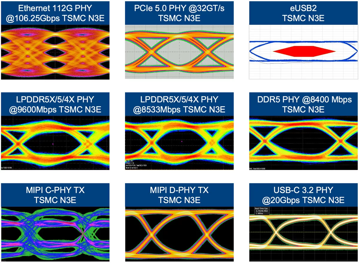
Synopsys Interface IP performs at blistering speeds with wide open eyes and clear margins
112G LR-Max PHY IP
As the image above illustrates, Synopsys 12G LR-Max PHY IP on TSMC's N3E process demonstrates highly linear PAM-4 eyes with excellent SNDR and jitter performance. Using leading-edge analog mixed-signal design and advanced digital signal processing (DSP) technologies, the 112G LR-Max PHY IP provides additional margins to the CEI-112G LR specification and delivers three orders of magnitude better bit error rate compared to the spec for 45dB channels. The Synopsys Multi-Protocol 112G PHY IP is part of our high-performance multi-rate transceiver portfolio for high-end networking and HPC applications.
PCIe 5.0 PHY IP
Running at 32 GT/s with clear, wide-open eyes, Synopsys PCIe 5.0 PHY IP on TSMC's N3E process successfully passed PCI-SIG 5.0 compliance testing and was the first IP to be listed on the 5.0 Integrators List. Synopsys' complete IP solution for PCIe consists of silicon-proven digital controllers, PHYs, Integrity and Data Encryption (IDE) Security Modules, and verification IP. As the leading supplier of IP solutions for PCIe, Synopsys enables cloud computing, storage, and AI accelerators to achieve low-latency, high-bandwidth requirements for real-time data connectivity.
DDR5 PHY IP
DDR is the de facto technology for system designs that require the highest capacity off-chip memory. That's why Synopsys DDR5 PHY IP on TSMC's N3E process operates up to 8400Mbps�supporting the JEDEC standard DDR5 SDRAMs and memory modules that enable workload-intensive server, enterprise, AI, and networking applications. First-pass silicon success on TSMC's N3E process helps customers design high-performance memory solutions with faster time to market and reduced integration risks. Synopsys DDR5 PHY IP is part of the complete Synopsys DDR interface solution that includes PHYs, controllers, secure inline memory encryption (IME), IP subsystems, verification IP, and IP Prototyping Kits.
LPDDR5X/4/4X IP
The Synopsys LPDDR5X/4/4X PHY IP tape out on TSMC's N3E process shows wide eyes and clear margins at 8533 Mbps and 9600 Mbps (overclocked). Optimized for power, latency, bandwidth, and area, the next-gen controller supports JEDEC standard LPDDR5X, LPDDR5, and LPDDR4X SDRAMs�and seamlessly integrates with the Synopsys Inline Memory Encryption (IME) Security Module to provide confidentiality of data in-use or stored in off-chip memory.
MIPI C-PHY/D-PHY IP
Running at a blistering 44Gbps, Synopsys MIPI C-PHY/D-PHY RX IP on TSMC's N3E process receives high-resolution image sensor traffic up to 6.5Gbps per trio in C-PHY mode and 6.5Gbps per lane in D-PHY mode. Part of the complete Synopsys MIPI solution, the MIPI C-PHY/D-PHY RX IP offers seamless interoperability with Synopsys' ASIL B-Ready, ISO 26262-certified CSI-2 and DSI/DSI-2 controllers for automotive cameras, sensors, and displays that enable advanced driver-assistance systems (ADAS). The MIPI C-PHY/D-PHY RX IP also supports high-performance, low-power interfaces for SoCs and peripheral devices used in mobile, AI, and IoT applications.
USB-C 3.2/DisplayPort 1.4 IP
Synopsys USB-C 3.2 and DisplayPort 1.4a IP on TSMC's N3E process delivers a blazing 20Gbps for USB-C 3.2, 32 Gbps for DP 1.4a, or simultaneous 10Gbps for USB plus 16Gbps DP 1.4a. The IP can be seamlessly integrated into SoCs that support connections to high-definition (HD), 2K, 4K, and 8K Ultra High Definition (UHD) displays for mobile devices, set-top boxes and other applications requiring fast data transfers and output of high-resolution content. To minimize design cycles, Synopsys offers complete solutions for USB/DisplayPort IP implementation, including PHYs, controllers, verification IP, and IP subsystems.
eUSB2 IP
Synopsys Embedded eUSB2 (eUSB2) PHYs on TSMC's N3E process targets low-power mobile and consumer products such as smartphones, tablets, laptops, gaming, AR/VR, and wireless devices. eUSB2 PHY IP enables USB 2.0 connectivity using 1V or 1.2V I/O voltage in the SoC, with legacy USB 2.0 3.3V signaling provided by an external Synopsys eUSB2 repeater.
Universal Chiplet Interconnect Express (UCIe) PHY IP
In addition to the above, Synopsys recently announced a successful tape out of Universal Chiplet Interconnect Express� (UCIe�) PHY IP on TSMC's N3E process. UCIe IP is a key element of multi-die systems, allowing chip designers to achieve secure and robust die-to-die connectivity in a package while delivering high bandwidth, low power, and low latency. The Synopsys UCIe PHY IP offers a flexible architecture that supports advanced and standard packaging technologies, providing up to 5Tbps/mm bandwidth efficiency. Synopsys UCIe Controller IP supports popular protocols such as PCI Express and CXL and enables secure, low-latency NoC-to-NoC links with streaming protocols.
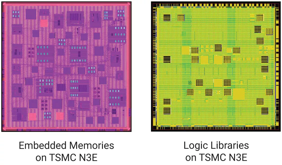
Foundation IP on 3nm
Synopsys also offers Foundation IP for TSMC's N3E process to help chip designers optimize silicon designs with embedded memories, logic libraries, and:
- Memory compilers
- High-performance core (HPC) design kits
- Power optimization kits (POK) and engineering change order (ECO) kits
Synopsys Foundation IP on advanced TSMC process technologies is extensively proven in silicon, with billions of units shipping in volume production.
Conclusion
Designing monolithic system-on-chips (SoCs) and multi-die systems on the most advanced processes offers many real-world benefits, from faster speeds and longer battery life to support for immersive user experiences, AI engines, and smarter devices. However, the laws of semiconductor physics aren't keeping pace with the demands of increasing silicon complexity, making it challenging for chip designers to efficiently meet ambitious design targets. Synopsys Foundation and Interface IP on TSMC's N3E process enables semiconductor companies to jumpstart 3nm chip designs, optimize their silicon, and accelerate time to market.